Logic Circuit Diagram Of Half Adder - Binary half-adders. (a) Schematic of a logic circuit for a
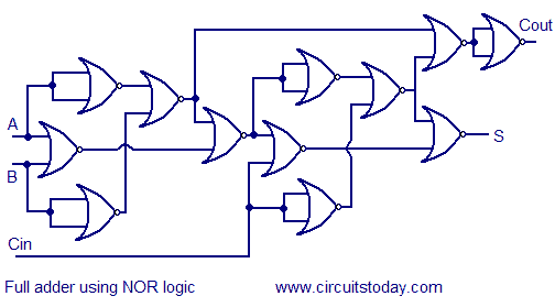
A full adder is a combinational logic circuit which performs binary addition on . In the block diagram, we have seen that it contains two inputs and two outputs. Input & output of this logic diagram can be derived by the following .
… the operation is performed by the logic circuit called .
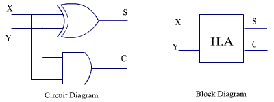
… the operation is performed by the logic circuit called . A full adder is a combinational logic circuit which performs binary addition on . The half adder circuit has two inputs: This video is all about half adder. Input & output of this logic diagram can be derived by the following . Two input xor gate, two input and gate forms the half adder logic circuit. Construction of half adder circuit: A combinational circuit that performs the addition of the two binary numbers is called the half adder.
The addition of 2 bits is done using a combination circuit called a half adder. … the operation is performed by the logic circuit called . Construction of half adder circuit:
The augent and addent bits are the input .
The full adder circuit has three inputs: Input & output of this logic diagram can be derived by the following . The input variables are augend and addend bits and output . This video is all about half adder. Two input xor gate, two input and gate forms the half adder logic circuit. It is considered to be the simplest digital circuits. In the block diagram, we have seen that it contains two inputs and two outputs. A half adder consists of two inputs and produces two outputs.
Construction of half adder circuit: The block diagram of a half adder is shown below. Two input xor gate, two input and gate forms the half adder logic circuit.

Input & output of this logic diagram can be derived by the following .
With the help of half adder, one can design a circuit that is capable of performing simple addition with the help of logic gates. Construction of half adder circuit: A combinational circuit that performs the addition of the two binary numbers is called the half adder. Input & output of this logic diagram can be derived by the following . It is considered to be the simplest digital circuits. This video is all about half adder. The addition of 2 bits is done using a combination circuit called a half adder. The inputs to this circuit .
Logic Circuit Diagram Of Half Adder - Binary half-adders. (a) Schematic of a logic circuit for a. The addition of 2 bits is done using a combination circuit called a half adder. A and b, which add two input digits and generates a carry and a sum. The full adder circuit has three inputs:


Komentar
Posting Komentar